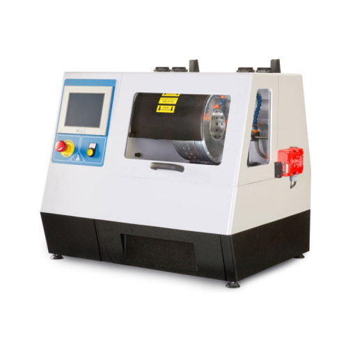
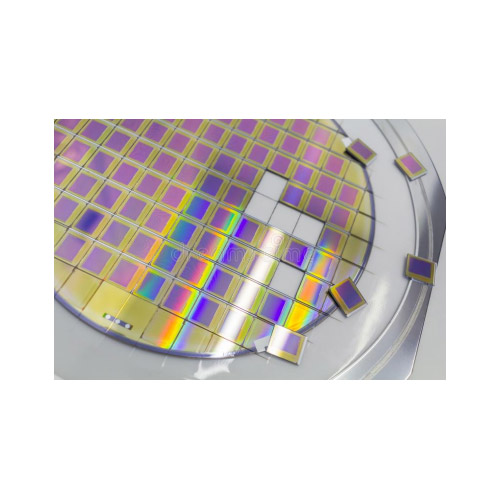
Offering the option of a unique combination of annular cutting and peripheral cutting capabilities in a precision saw, the cutting of semiconductor wafers from the crystal boule and subsequent cutting into substrates can take place in one unit.
APD1 is designed to allow samples to be cut and sliced accurately and finely with minimal surface damage and loss of kerf. Programmed automatic operation allows repeated cuts to be made to selected thicknesses and diameters, allowing for completely autonomous operation.
The saw is easily operated using defined parameters, such as depth of cut, thickness of cut and the number of cuts to be made.
The APD1 precision saw is an effective tool in applications such as:
- Cut and crystal wafer
- Electronic components sectioning
- Cutting semiconductor components
- Deep fitting
Ideal for cutting a wide range of glass, ceramics, rock samples and electro-optical materials.
Applicable for silicon, lithium niobate, lithium tantalate, bismuith silicon oxide, barium titanate and similar materials. Whether for producing infrared and polymer waveguide or polishing fiber optic cable.
Semiconductor materials are used in a wide variety of devices, such as field effect transistors (MosFets, Fets), integrated circuits (ICs, MMICs, ASICs), focal plane arrays and infrared detectors.


